Next generation of Thermo-Compression Bonding Equipment
Jonathan Abdilla, Martin Kainz, Benedikt Pressl, Mario Fraubaum, Chris Scanlan.
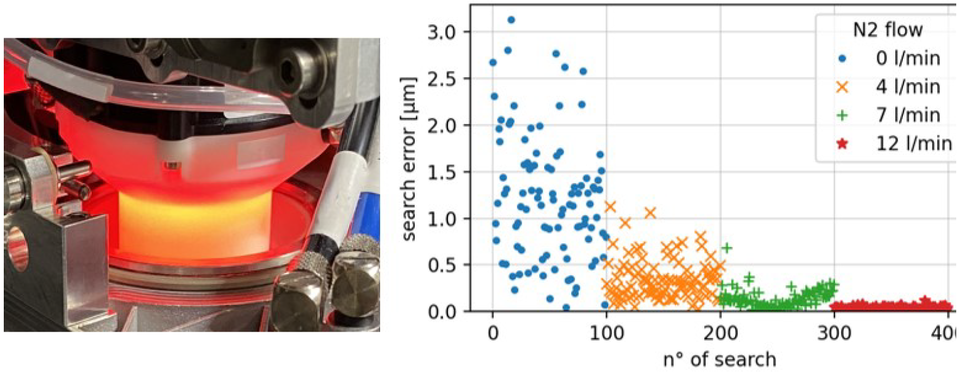
As transistor technology node scaling slows down, alternative approaches are being explored to sustain the momentum of Moore’s law. Chip sizes have now reached reticle limits, posing challenges for adding more features. Additionally, large dies come with their own set of disadvantages, including reduced yield, longer time to market, increased complexity, higher design and engineering costs, limited flexibility for customization, and an inability to utilize different nodes for various architectures to reduce costs. While material selection is a critical aspect which can help, packaging has more prominently taken the spotlight. A stateof-the-art thermocompression bonding (TCB) equipment has been proven to achieve sub micron accuracy, and implementation of a no flux TCB process with hydroxyl reduction proven via cross sectioning of specimens. Innovative ways to deal with search inaccuracies performed by cameras induced from elevated temperatures are also presented with nm repeatability.
Download the full article below.
Thermo compression bonding for large dies under protective atmosphere

Jonathan Abdilla, Uwe Bayer, Ruurd Boomsma, Stephan Bulacher, Alexander Kalss, Stephan Martin, Harald Meixner, Thiago Moura, Hubert Selhofer, Wolfgang Voegele, Martin Widauer.
In bond pitch ranges of 50 to 30 micrometer Thermo Compression Bonding (TCB) is an established bonding technology for example for high bandwidth memory (HBM) using relative small dies. For logic, processor and interposer applications, die sizes may be much larger and bonding behavior may be more complicated due to warpage, relative high heater powers, high number of contacts and possible oxidation issues. This paper will describe bonding behavior for up to 80mm x 80mm die sizes including methods using protective/reduction gas during bonding with extreme low gas consumption and effective oxidation prevention.
Download the full article below.
Die-to-wafer hybrid bonding development for High Volume Manufacturing
Jonathan Abdilla Et al.
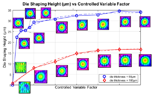
As the demands of high-performance computing (HPC) and artificial intelligence (AI) grow, traditional semiconductor packaging methods like flip-chip bonding face limitations in scalability and reliability. This article explores the advanced die-to-wafer (D2W) hybrid bonding process, which offers significant improvements by using copper-to-copper (Cu-Cu) connections. We will discuss key process steps, such as wet cleaning, degassing, and plasma surface treatment, and present data on Cu-Cu diffusion, void formation, and placement accuracy. This comprehensive overview highlights how D2W hybrid bonding enhances system-level performance and is essential for high-volume manufacturing in advanced semiconductor packaging.
Download the full article below.
Materials and solutions for power package die bonding
Jonathan Abdilla Et al.
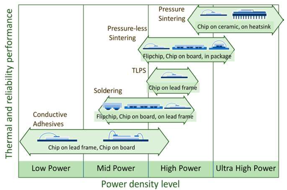
Power electronics packaging is evolving rapidly to meet the growing demand in applications like automotive, consumer electronics, and renewable energy. These advancements are driven by the need for improved power density, thermal management, reliability, and cost-efficiency. This article explores major die bonding techniques used in power packaging, including soft-solder die attach, conductive adhesives, and the increasingly popular sintering methods. By comparing these technologies, we aim to provide a clearer understanding of their benefits and limitations, helping engineers choose the best solutions for high-performance, high-reliability applications.
High-Accuracy Pick-and-Place of Multiple Dies in Parallel Assisted by Capillary Self-Alignment
Birgit Brandstätter Et al.
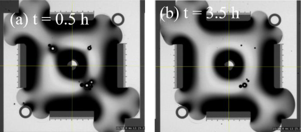
Self-assembly of components driven by liquid surface tension is an attractive complement and even alternative to traditional high-accuracy pick-and-place as it offers high accuracy despite inaccurate robotic part placement. While capillary self-alignment through liquid solder is the standard technology for flip-chip processes, this work presents self-alignment of dies on wetted receptors on a temporary carrier: Low-viscosity liquid is jetted on each receptor where the liquid is contained through generation of hydrophilic and hydrophobic sections on the temporary carrier by plasma treatment. Deterministic die feeding by low-accuracy pick-and-place is conducted for single dies, as well as for batches of three dies and nine dies optimizing the equipment for best throughput to achieve both high accuracy and high productivity. The industry-ready and fully automated chip-to-wafer pick-and-place process is implemented into a fan-out wafer-level packaging production flow proving that self-alignment is capable of easing the stringent requirement for robotic alignment capability for pick-and-place systems in fan-out packaging for the single die-level step in this production chain. The self-alignment process is optimized, and failure modes such as poor liquid confinement, surface contamination, or excess force are identified and eliminated. Post-bond accuracy of <3 μm @ 3 σ at each point of the die is reached for dies of 3.1 mm x 3.1 mm in size. Using parallel die handling, high speeds of around 10 000 units per hour are made possible.
Download the full paper below.
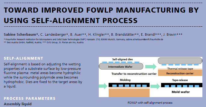
Toward improved FOWLP manufacturing by using self-alignment process
December 2020 - Birgit Brandstätter Et al.
Together with the Frauhofer Institute, a poster with the title Toward improved FOWLP manufacturing by using self-alignment process was made.
Self-alignment is based on adjusting the wetting properties of a substrate surface by low-pressure fluorine plasma: metal areas become hydrophilic while the surrounding polyimide area becomes hydrophobic. Dies are fixed to the target areas by a liquid.
Download the poster below.
High-speed ultra-accurate direct C2W bonding
Birgit Brandstätter Et al.
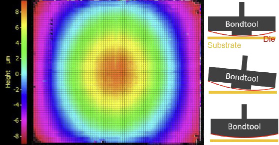
Chip-to-wafer hybrid bonding is needed as contact pitch and pad size decrease to the single micrometer range (5 micrometer or lower). Here, classical bonding technologies like themo-compression bonding and flip-chip with mass reflow are no longer sufficient, and hybrid bonding emerges as an attractive alternative. While the technology is well known in wafer-to-wafer processing, for chip-to-wafer at industrial speed and accuracy, new placement technologies and deeper understanding of accuracy behavior during the bonding process both are essential. This paper describes new optical recognition methods for small pads for accurate in-situ alignment before the bonding stroke as well as a new bond-head design and behavior for accurate placement at 200 nm at each point of the die, including large dies, and at speeds of 2000 units per hour.
Download the full paper below.
Contact
Besi Netherlands B.V.
Tel: +31 26 319 6100
Besi Switzerland AG
Tel: +41 41 749 5111
Besi Austria GmbH
Tel: +43 5337 6000
Meco Equipment Engineers B.V.
Tel: +31 416 384 384
