Datacon 2200 evo
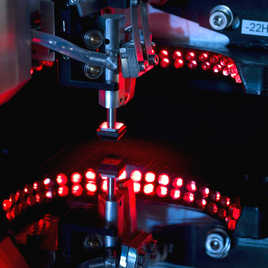
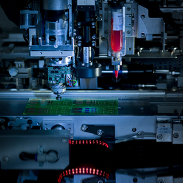
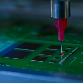
The Datacon 2200 evo high-accuracy multi-chip die bonder provides the ultimate flexibility for die attach as well as for flip chip applications. Equipped with integrated dispenser, 12” wafer handling, automatic tool changer, and application specific tooling, the Datacon 2200 evo is prepared for present and future processes and products.
Key Features
High Performance at High Accuracy
- Highest accuracy ± 10 µm @ 3 Sigma (7 µm on request)
- High productivity, low cost-of-ownership
- Up to 4 working heads in one machine
Multi-Chip Capability
- Single pass production for complex products
- Die attach, flip chip, multi-chip in one machine
- Epoxy writing & stamping, flux dipping
Unbeaten Flexibility
- Die pick from wafer, waffle pack, gel pack, feeder
- Die place to carrier, boat, substrate, PCB, lead frame, wafer
- Hot and cold processes supported: epoxy, soldering, thermo-compression
- MCM, SiP, Hybrids
Open Platform Architecture for Full Customization
- Most advanced modular platform concept
- Production line tailored 100% to your needs
- Ideal solution with smallest footprint possible
Specifications
Performance
- X/Y placement accuracy: ± 10 µm @ 3s
- Theta placement accuracy: ± 0.15° @ 3s
- Bond Force: 0.5N to 75N programmable
UPH
- Die attach: up to 7,000 UPH/module
- Flip Chip with dipping: up to 2,500 UPH/module
- Flip Chip without dipping: up to 3,200 UPH/module
Bond Heads
- Standard bond head 0° - 360° rotation
- Heated bond head up to 450°C (optional)
- UV Curing (365 nm & 405 nm)
Machine Dimensions
- LxDxH: 1,160 mm x 1,225 mm x 1,750 mm
- Weight: 1,300 kg
Statistics
- Uptime > 98 %
- Yield > 99.95 %
Wafer
- Die size Die Attach: 0.17 mm - 50 mm
- Die size Flip Chip: 0.5 mm - 50 mm
- Die thickness: >50 µm (thinner on request)
- Wafer size: 4" - 12" (SEMI M1)
- Frame size: FF070, FF105, FF108, FF123; automatic change (others on request)
Chip Trays
- Waffle pack / Gel-Pak® 2” x 2” and 4” x 4”
- JEDEC tray on request
Substrates and Carriers
- FR4, ceramic, BGA, flex, boat, lead frame, waffle pack
- Gel-Pak®, JEDEC tray, odd-shape substrates
- Substrate working range: 13” x 8” (325 mm x 200 mm)
Options
- Hardware: Open platform architecture for full customization
- Software: Single component tracking, CAD download, wafer mapping, substrate mapping, barcode scanner, datamatrix recognition and more
Downloads
PDF - 2 MB


